Technical Information
Home
AM Basics & Station Setup
Class E Overview and
Theory of Operation
Output Circuit Values & MOSFET ratings
High Power & Harmonic Reduction
Device Protection
Testing & Tuning Procedures
Modulators & Power Supplies
Design Tools
Construction Projects
Construction Overview
Simple 400 Watt
RF Amp for
80 meters
VFO for 160 & 80 meters
Using a lower power
transmitter as an
RF source (A to D converter)
Pulse Width Modulator and power supply
24 MOSFET RF Amplifier - Step by Step
Analog Modulator (Class H) and power supply
Overall Schematic of a complete modulator/power supply
Class E Kits
and Parts

Technical Support
|
.
|
|| Class E Home
|| WA1QIX home page
|| QuickEasy Logger Page
|| Class E Forum
|| AMFone
||
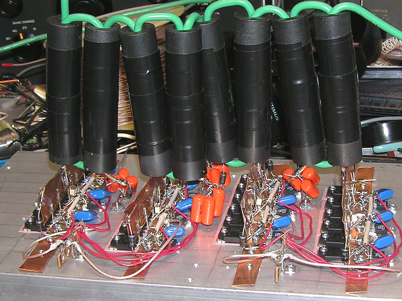
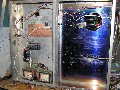
This is a 24 MOSFET Class E RF Amplifier, covering the 80 and 160 meter amateur radio bands.
The amplifier is constructed in 4 6-MOSFET modules and uses IXDD414 digital gate drivers. Each gate driver drives 2 MOSFETs.
A single 1500pF multilayer ceramic capacitor is used per module as the shunt capacitor when operaing on 80 meters.
An additional 1500pF capacitor is switched in (using small relays) when operating on the 160 meter band.
2 coils are used, one for 80 meters and an additional coil for 160 meters, which is shorted out by a relay when operating on 80 meters.
The tuning capacitor has sufficient range to cover both bands. 2 loading capacitors are used to provide sufficient capacitance for 160 meters.
A fixed capacitor could also be used, if the device can handle the high RF current.
Schematics:
Pictures of the various construction steps for the 24 MOSFET RF Amplifier
Click on any picture to see a bigger image.
|
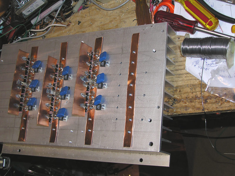
The Beginning Phases of Construction
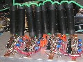
Heat sink drilled with some parts mounted.

The source bus ready to be soldered to the MOSFET sources.
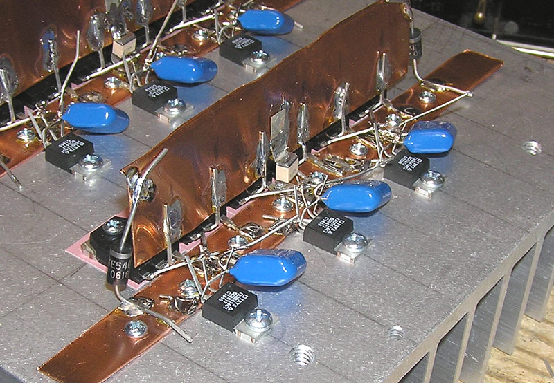
Good closeup of a module showing the drain bus and shunt capacitor.
The drivers are mounted, ready to be soldered.
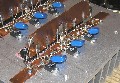
Drivers soldered to gate pins, driver bypass caps, drain transzorbs.
|
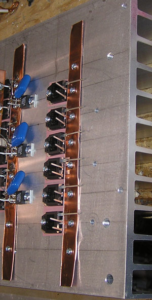
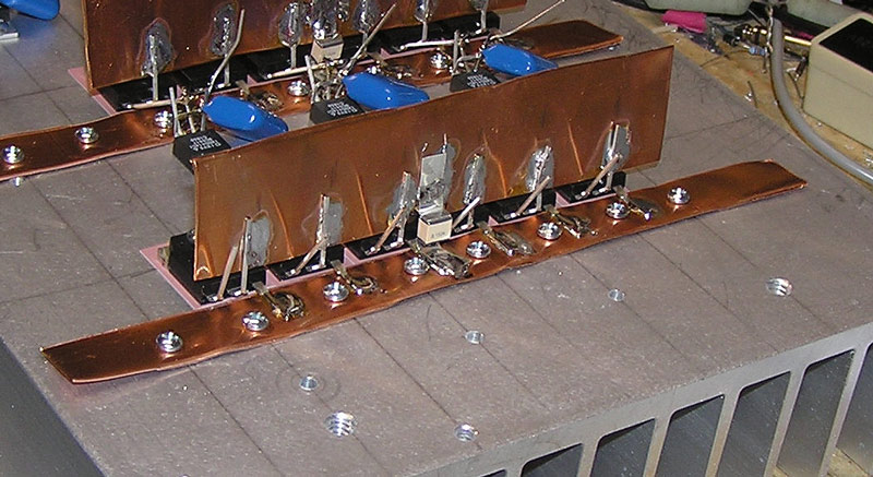
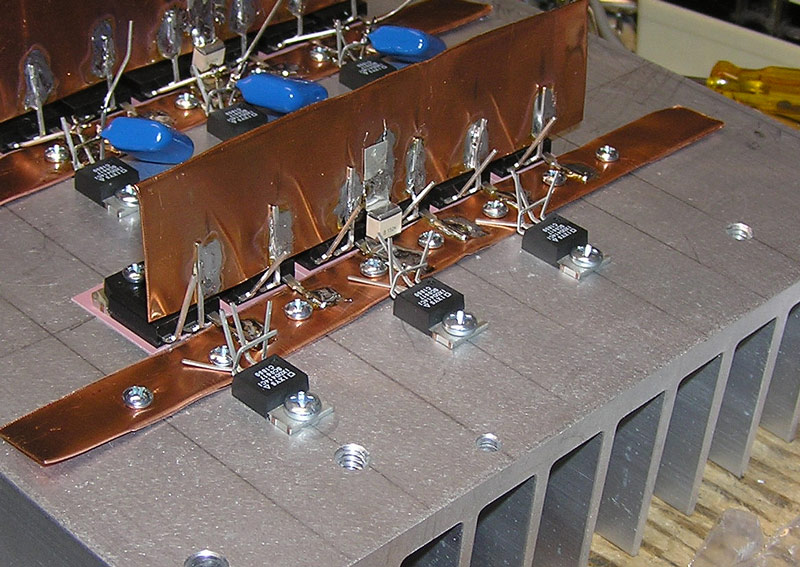
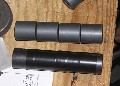
Further into the construction
Closeup of the drivers, terminating resistors and connections to the driver input pins.
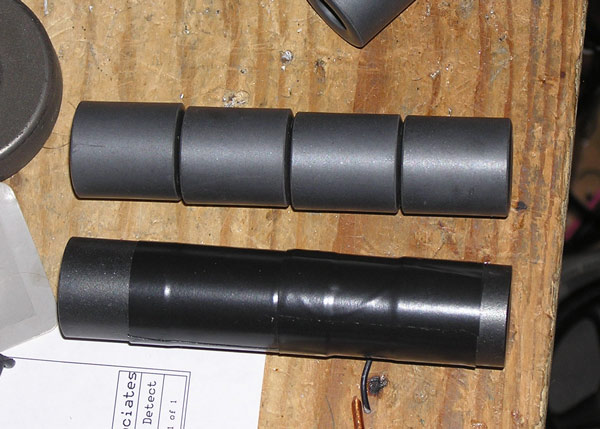
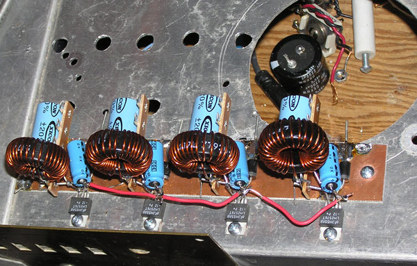
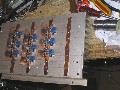
Starting the output transformers (1:1 ratio).
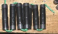
The secondary winding is run through the cores first.
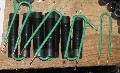
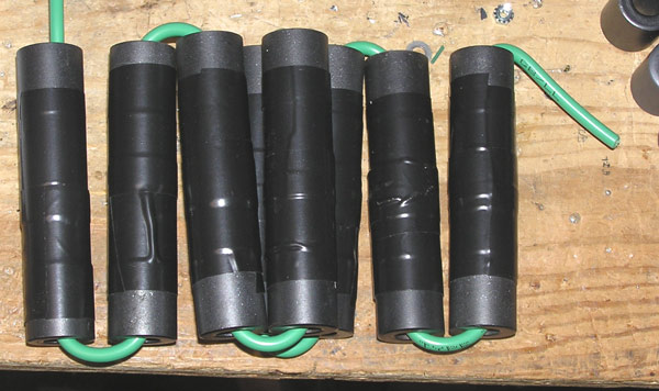
The primary windows are cut and bent. They should all be exactly the same.

The primary windows are inserted into the cores to form transformers.
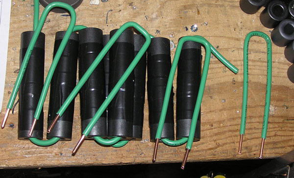
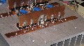
A good shot showing all of the transformer connections. It is very important
for the transformers to be connected properly to ensure proper combination of
the class E modules.
|
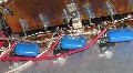
Finally Assembly and Completion
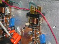
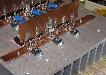
Closeup showing the shunt capacitor bandswitch relays. The shunt capacitors are
soldered directly to the relays, and the relays are soldered to the drain bus through a piece of copper. This is done
to minimize the inductance in the shunt capacitor path to ground.
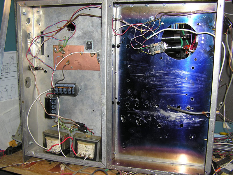
In my implementation, each module has its own 12V switching regulator for the drivers. You do not have to
build it this way. You can use a single 12V 15A supply or thereabouts, and it will work just fine. The 12V supply
for the drivers may be left on all the time. It does not need to be switched off between transmissions, and is probably
best left on.
The underside showing the driver power supply transformers.
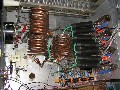
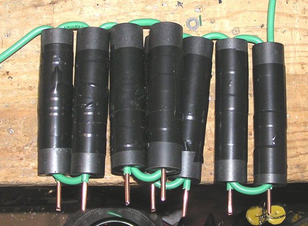
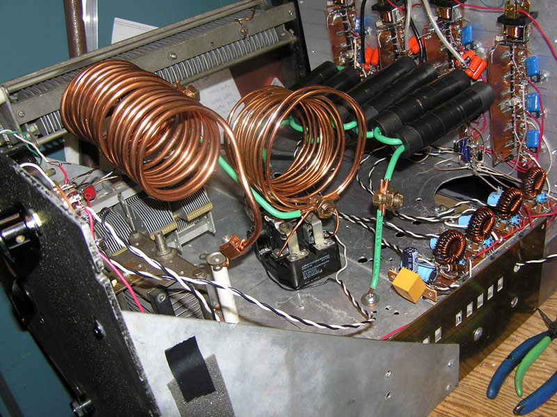
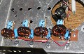
View of the RF deck from the top. The 160 meter coil is to the right, and
the 160 meter coil relay is visible just underneath the 160 meter coil.
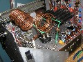
Another view of the completed RF deck. The variable capacitor to the far right
is an additional loading capacitor in parallel with the main loading capacitor.
|
|